A | B | C | D | E | F | G | H | CH | I | J | K | L | M | N | O | P | Q | R | S | T | U | V | W | X | Y | Z | 0 | 1 | 2 | 3 | 4 | 5 | 6 | 7 | 8 | 9
This article has an unclear citation style. (April 2019) |
| Computer memory and Computer data storage types |
|---|
| Volatile |
| Non-volatile |


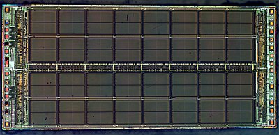
Dynamic random-access memory (dynamic RAM or DRAM) is a type of random-access semiconductor memory that stores each bit of data in a memory cell, usually consisting of a tiny capacitor and a transistor, both typically based on metal–oxide–semiconductor (MOS) technology. While most DRAM memory cell designs use a capacitor and transistor, some only use two transistors. In the designs where a capacitor is used, the capacitor can either be charged or discharged; these two states are taken to represent the two values of a bit, conventionally called 0 and 1. The electric charge on the capacitors gradually leaks away; without intervention the data on the capacitor would soon be lost. To prevent this, DRAM requires an external memory refresh circuit which periodically rewrites the data in the capacitors, restoring them to their original charge. This refresh process is the defining characteristic of dynamic random-access memory, in contrast to static random-access memory (SRAM) which does not require data to be refreshed. Unlike flash memory, DRAM is volatile memory (vs. non-volatile memory), since it loses its data quickly when power is removed. However, DRAM does exhibit limited data remanence.
DRAM typically takes the form of an integrated circuit chip, which can consist of dozens to billions of DRAM memory cells. DRAM chips are widely used in digital electronics where low-cost and high-capacity computer memory is required. One of the largest applications for DRAM is the main memory (colloquially called the "RAM") in modern computers and graphics cards (where the "main memory" is called the graphics memory). It is also used in many portable devices and video game consoles. In contrast, SRAM, which is faster and more expensive than DRAM, is typically used where speed is of greater concern than cost and size, such as the cache memories in processors.
The need to refresh DRAM demands more complicated circuitry and timing than SRAM. This is offset by the structural simplicity of DRAM memory cells: only one transistor and a capacitor are required per bit, compared to four or six transistors in SRAM. This allows DRAM to reach very high densities with a simultaneous reduction in cost per bit. Refreshing the data consumes power and a variety of techniques are used to manage the overall power consumption.
DRAM had a 47% increase in the price-per-bit in 2017, the largest jump in 30 years since the 45% jump in 1988, while in recent years the price has been going down.[3] In 2018, a "key characteristic of the DRAM market is that there are currently only three major suppliers — Micron Technology, SK Hynix and Samsung Electronics" that are "keeping a pretty tight rein on their capacity".[4] There is also Kioxia (previously Toshiba Memory Corporation after 2017 spin-off). Other manufacturers make and sell DIMMs (but not the DRAM chips in them), such as Kingston Technology, and some manufacturers that sell stacked DRAM (used e.g. in the fastest supercomputers on the exascale), separately such as Viking Technology. Others sell such integrated into other products, such as Fujitsu into its CPUs, AMD in GPUs, and Nvidia, with HBM2 in some of their GPU chips.
History

The cryptanalytic machine code-named "Aquarius" used at Bletchley Park during World War II incorporated a hard-wired dynamic memory. Paper tape was read and the characters on it "were remembered in a dynamic store. ... The store used a large bank of capacitors, which were either charged or not, a charged capacitor representing cross (1) and an uncharged capacitor dot (0). Since the charge gradually leaked away, a periodic pulse was applied to top up those still charged (hence the term 'dynamic')".[5]
Toshiba invented and introduced a dynamic RAM for its electronic calculator "Toscal" BC-1411, which was introduced in November 1965;[6][7] it used a form of capacitive DRAM (180 bit) built from discrete bipolar memory cells.[6][8]
In 1967, Tomohisa Yoshimaru and Hiroshi Komikawa from Toshiba applied for an American patent of the concept with a priority of May, 1966 due to an early Japanese application.[9]
The earliest forms of DRAM mentioned above used bipolar transistors. While it offered improved performance over magnetic-core memory, bipolar DRAM could not compete with the lower price of the then-dominant magnetic-core memory.[10] Capacitors had also been used for earlier memory schemes, such as the drum of the Atanasoff–Berry Computer, the Williams tube and the Selectron tube. In 1966, Dr. Robert Dennard at the IBM Thomas J. Watson Research Center was working on MOS memory and was trying to create an alternative to SRAM which required six MOS transistors for each bit of data. While examining the characteristics of MOS technology, he found it was capable of building capacitors, and that storing a charge or no charge on the MOS capacitor could represent the 1 and 0 of a bit, while the MOS transistor could control writing the charge to the capacitor. This led to his development of the single-transistor MOS DRAM memory cell.[11] He filed a patent in 1967, and was granted U.S. patent number 3,387,286 in 1968.[12] MOS memory offered higher performance, was cheaper, and consumed less power, than magnetic-core memory.[13]
MOS DRAM chips were commercialized in 1969 by Advanced Memory Systems, Inc of Sunnyvale, CA. This 1024 bit chip was sold to Honeywell, Raytheon, Wang Laboratories, and others. The same year, Honeywell asked Intel to make a DRAM using a three-transistor cell that they had developed. This became the Intel 1102 in early 1970.[14] However, the 1102 had many problems, prompting Intel to begin work on their own improved design, in secrecy to avoid conflict with Honeywell. This became the first commercially available DRAM, the Intel 1103, in October 1970, despite initial problems with low yield until the fifth revision of the masks. The 1103 was designed by Joel Karp and laid out by Pat Earhart. The masks were cut by Barbara Maness and Judy Garcia.[15][original research?] MOS memory overtook magnetic-core memory as the dominant memory technology in the early 1970s.[13]
The first DRAM with multiplexed row and column address lines was the Mostek MK4096 4 Kbit DRAM designed by Robert Proebsting and introduced in 1973. This addressing scheme uses the same address pins to receive the low half and the high half of the address of the memory cell being referenced, switching between the two halves on alternating bus cycles. This was a radical advance, effectively halving the number of address lines required, which enabled it to fit into packages with fewer pins, a cost advantage that grew with every jump in memory size. The MK4096 proved to be a very robust design for customer applications. At the 16 Kbit density, the cost advantage increased; the 16 Kbit Mostek MK4116 DRAM,[16][17] introduced in 1976, achieved greater than 75% worldwide DRAM market share. However, as density increased to 64 Kbit in the early 1980s, Mostek and other US manufacturers were overtaken by Japanese DRAM manufacturers, which dominated the US and worldwide markets during the 1980s and 1990s.
Early in 1985, Gordon Moore decided to withdraw Intel from producing DRAM.[18] By 1986, many, but not all, United States chip makers had stopped making DRAMs.[19] Micron Technology and Texas Instruments continued to produce them commercially, and IBM produced them for internal use.
In 1985, when 64K DRAM memory chips were the most common memory chips used in computers, and when more than 60 percent of those chips were produced by Japanese companies, semiconductor makers in the United States accused Japanese companies of export dumping for the purpose of driving makers in the United States out of the commodity memory chip business. Prices for the 64K product plummeted to as low as 35 cents apiece from $3.50 within 18 months, with disastrous financial consequences for some U.S. firms. On 4 December 1985 the US Commerce Department's International Trade Administration ruled in favor of the complaint.[20]
Synchronous dynamic random-access memory (SDRAM) was developed by Samsung. The first commercial SDRAM chip was the Samsung KM48SL2000, which had a capacity of 16 Mb,[21] and was introduced in 1992.[22] The first commercial DDR SDRAM (double data rate SDRAM) memory chip was Samsung's 64 Mb DDR SDRAM chip, released in 1998.[23]
Later, in 2001, Japanese DRAM makers accused Korean DRAM manufacturers of dumping.[24]
In 2002, US computer makers made claims of DRAM price fixing.
Principles of operation


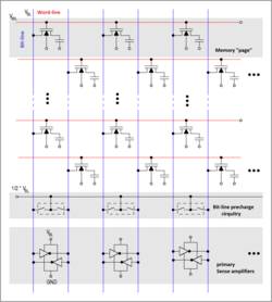
DRAM is usually arranged in a rectangular array of charge storage cells consisting of one capacitor and transistor per data bit. The figure to the right shows a simple example with a four-by-four cell matrix. Some DRAM matrices are many thousands of cells in height and width.[25][26]
The long horizontal lines connecting each row are known as word-lines. Each column of cells is composed of two bit-lines, each connected to every other storage cell in the column (the illustration to the right does not include this important detail). They are generally known as the "+" and "−" bit lines.
A sense amplifier is essentially a pair of cross-connected inverters between the bit-lines. The first inverter is connected with input from the + bit-line and output to the − bit-line. The second inverter's input is from the − bit-line with output to the + bit-line. This results in positive feedback which stabilizes after one bit-line is fully at its highest voltage and the other bit-line is at the lowest possible voltage.
Operations to read a data bit from a DRAM storage cell
- The sense amplifiers are disconnected.[27]
- The bit-lines are precharged to exactly equal voltages that are in between high and low logic levels (e.g., 0.5 V if the two levels are 0 and 1 V). The bit-lines are physically symmetrical to keep the capacitance equal, and therefore at this time their voltages are equal.[27]
- The precharge circuit is switched off. Because the bit-lines are relatively long, they have enough capacitance to maintain the precharged voltage for a brief time. This is an example of dynamic logic.[27]
- The desired row's word-line is then driven high to connect a cell's storage capacitor to its bit-line. This causes the transistor to conduct, transferring charge from the storage cell to the connected bit-line (if the stored value is 1) or from the connected bit-line to the storage cell (if the stored value is 0). Since the capacitance of the bit-line is typically much higher than the capacitance of the storage cell, the voltage on the bit-line increases very slightly if the storage cell's capacitor is discharged and decreases very slightly if the storage cell is charged (e.g., 0.54 and 0.45 V in the two cases). As the other bit-line holds 0.50 V there is a small voltage difference between the two twisted bit-lines.[27]
- The sense amplifiers are now connected to the bit-lines pairs. Positive feedback then occurs from the cross-connected inverters, thereby amplifying the small voltage difference between the odd and even row bit-lines of a particular column until one bit line is fully at the lowest voltage and the other is at the maximum high voltage. Once this has happened, the row is "open" (the desired cell data is available).[27]
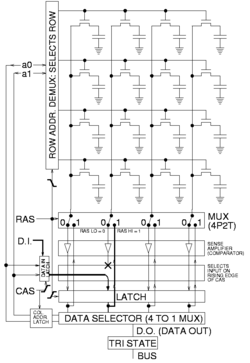
- All storage cells in the open row are sensed simultaneously, and the sense amplifier outputs latched. A column address then selects which latch bit to connect to the external data bus. Reads of different columns in the same row can be performed without a row opening delay because, for the open row, all data has already been sensed and latched.[27]
- While reading of columns in an open row is occurring, current is flowing back up the bit-lines from the output of the sense amplifiers and recharging the storage cells. This reinforces (i.e. "refreshes") the charge in the storage cell by increasing the voltage in the storage capacitor if it was charged to begin with, or by keeping it discharged if it was empty. Note that due to the length of the bit-lines there is a fairly long propagation delay for the charge to be transferred back to the cell's capacitor. This takes significant time past the end of sense amplification, and thus overlaps with one or more column reads.[27]
- When done with reading all the columns in the current open row, the word-line is switched off to disconnect the storage cell capacitors (the row is "closed") from the bit-lines. The sense amplifier is switched off, and the bit-lines are precharged again.[27]
To write to memory

To store data, a row is opened and a given column's sense amplifier is temporarily forced to the desired high or low voltage state, thus causing the bit-line to charge or discharge the cell storage capacitor to the desired value. Due to the sense amplifier's positive feedback configuration, it will hold a bit-line at stable voltage even after the forcing voltage is removed. During a write to a particular cell, all the columns in a row are sensed simultaneously just as during reading, so although only a single column's storage-cell capacitor charge is changed, the entire row is refreshed (written back in), as illustrated in the figure to the right.[27]
Refresh rate
Typically, manufacturers specify that each row must be refreshed every 64 ms or less, as defined by the JEDEC standard.
Some systems refresh every row in a burst of activity involving all rows every 64 ms. Other systems refresh one row at a time staggered throughout the 64 ms interval. For example, a system with 213 = 8,192 rows would require a staggered refresh rate of one row every 7.8 μs which is 64 ms divided by 8,192 rows. A few real-time systems refresh a portion of memory at a time determined by an external timer function that governs the operation of the rest of a system, such as the vertical blanking interval that occurs every 10–20 ms in video equipment.
The row address of the row that will be refreshed next is maintained by external logic or a counter within the DRAM. A system that provides the row address (and the refresh command) does so to have greater control over when to refresh and which row to refresh. This is done to minimize conflicts with memory accesses, since such a system has both knowledge of the memory access patterns and the refresh requirements of the DRAM. When the row address is supplied by a counter within the DRAM, the system relinquishes control over which row is refreshed and only provides the refresh command. Some modern DRAMs are capable of self-refresh; no external logic is required to instruct the DRAM to refresh or to provide a row address.
Under some conditions, most of the data in DRAM can be recovered even if the DRAM has not been refreshed for several minutes.[28]
Memory timing
Many parameters are required to fully describe the timing of DRAM operation. Here are some examples for two timing grades of asynchronous DRAM, from a data sheet published in 1998:[29]


