A | B | C | D | E | F | G | H | CH | I | J | K | L | M | N | O | P | Q | R | S | T | U | V | W | X | Y | Z | 0 | 1 | 2 | 3 | 4 | 5 | 6 | 7 | 8 | 9


In electronics, an analog-to-digital converter (ADC, A/D, or A-to-D) is a system that converts an analog signal, such as a sound picked up by a microphone or light entering a digital camera, into a digital signal. An ADC may also provide an isolated measurement such as an electronic device that converts an analog input voltage or current to a digital number representing the magnitude of the voltage or current. Typically the digital output is a two's complement binary number that is proportional to the input, but there are other possibilities.
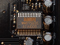
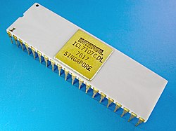
There are several ADC architectures. Due to the complexity and the need for precisely matched components, all but the most specialized ADCs are implemented as integrated circuits (ICs). These typically take the form of metal–oxide–semiconductor (MOS) mixed-signal integrated circuit chips that integrate both analog and digital circuits.
A digital-to-analog converter (DAC) performs the reverse function; it converts a digital signal into an analog signal.
Explanation
An ADC converts a continuous-time and continuous-amplitude analog signal to a discrete-time and discrete-amplitude digital signal. The conversion involves quantization of the input, so it necessarily introduces a small amount of quantization error. Furthermore, instead of continuously performing the conversion, an ADC does the conversion periodically, sampling the input, and limiting the allowable bandwidth of the input signal.
The performance of an ADC is primarily characterized by its bandwidth and signal-to-noise ratio (SNR). The bandwidth of an ADC is characterized primarily by its sampling rate. The SNR of an ADC is influenced by many factors, including the resolution, linearity and accuracy (how well the quantization levels match the true analog signal), aliasing and jitter. The SNR of an ADC is often summarized in terms of its effective number of bits (ENOB), the number of bits of each measure it returns that are on average not noise. An ideal ADC has an ENOB equal to its resolution. ADCs are chosen to match the bandwidth and required SNR of the signal to be digitized. If an ADC operates at a sampling rate greater than twice the bandwidth of the signal, then per the Nyquist–Shannon sampling theorem, near-perfect reconstruction is possible. The presence of quantization error limits the SNR of even an ideal ADC. However, if the SNR of the ADC exceeds that of the input signal, then the effects of quantization error may be neglected, resulting in an essentially perfect digital representation of the bandlimited analog input signal.
Resolution

The resolution of the converter indicates the number of different, i.e. discrete, values it can produce over the allowed range of analog input values. Thus a particular resolution determines the magnitude of the quantization error and therefore determines the maximum possible signal-to-noise ratio for an ideal ADC without the use of oversampling. The input samples are usually stored electronically in binary form within the ADC, so the resolution is usually expressed as the audio bit depth. In consequence, the number of discrete values available is usually a power of two. For example, an ADC with a resolution of 8 bits can encode an analog input to one in 256 different levels (28 = 256). The values can represent the ranges from 0 to 255 (i.e. as unsigned integers) or from −128 to 127 (i.e. as signed integer), depending on the application.
Resolution can also be defined electrically, and expressed in volts. The change in voltage required to guarantee a change in the output code level is called the least significant bit (LSB) voltage. The resolution Q of the ADC is equal to the LSB voltage. The voltage resolution of an ADC is equal to its overall voltage measurement range divided by the number of intervals:
where M is the ADC's resolution in bits and EFSR is the full-scale voltage range (also called 'span'). EFSR is given by
where VRefHi and VRefLow are the upper and lower extremes, respectively, of the voltages that can be coded.
Normally, the number of voltage intervals is given by
where M is the ADC's resolution in bits.[1]
That is, one voltage interval is assigned in between two consecutive code levels.
Example:
- Coding scheme as in figure 1
- Full scale measurement range = 0 to 1 volt
- ADC resolution is 3 bits: 23 = 8 quantization levels (codes)
- ADC voltage resolution, Q = 1 V / 8 = 0.125 V.
In many cases, the useful resolution of a converter is limited by the signal-to-noise ratio (SNR) and other errors in the overall system expressed as an ENOB.

Quantization error

Quantization error is introduced by the quantization inherent in an ideal ADC. It is a rounding error between the analog input voltage to the ADC and the output digitized value. The error is nonlinear and signal-dependent. In an ideal ADC, where the quantization error is uniformly distributed between −1⁄2 LSB and +1⁄2 LSB, and the signal has a uniform distribution covering all quantization levels, the signal-to-quantization-noise ratio (SQNR) is given by
where Q is the number of quantization bits. For example, for a 16-bit ADC, the quantization error is 96.3 dB below the maximum level.
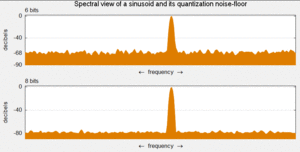
Quantization error is distributed from DC to the Nyquist frequency. Consequently, if part of the ADC's bandwidth is not used, as is the case with oversampling, some of the quantization error will occur out-of-band, effectively improving the SQNR for the bandwidth in use. In an oversampled system, noise shaping can be used to further increase SQNR by forcing more quantization error out of band.
Dither
In ADCs, performance can usually be improved using dither. This is a very small amount of random noise (e.g. white noise), which is added to the input before conversion. Its effect is to randomize the state of the LSB based on the signal. Rather than the signal simply getting cut off altogether at low levels, it extends the effective range of signals that the ADC can convert, at the expense of a slight increase in noise. Dither can only increase the resolution of a sampler. It cannot improve the linearity, and thus accuracy does not necessarily improve.
Quantization distortion in an audio signal of very low level with respect to the bit depth of the ADC is correlated with the signal and sounds distorted and unpleasant. With dithering, the distortion is transformed into noise. The undistorted signal may be recovered accurately by averaging over time. Dithering is also used in integrating systems such as electricity meters. Since the values are added together, the dithering produces results that are more exact than the LSB of the analog-to-digital converter.
Dither is often applied when quantizing photographic images to a fewer number of bits per pixel—the image becomes noisier but to the eye looks far more realistic than the quantized image, which otherwise becomes banded. This analogous process may help to visualize the effect of dither on an analog audio signal that is converted to digital.
Accuracy
An ADC has several sources of errors. Quantization error and (assuming the ADC is intended to be linear) non-linearity are intrinsic to any analog-to-digital conversion. These errors are measured in a unit called the least significant bit (LSB). In the above example of an eight-bit ADC, an error of one LSB is 1⁄256 of the full signal range, or about 0.4%.
Nonlinearity
All ADCs suffer from nonlinearity errors caused by their physical imperfections, causing their output to deviate from a linear function (or some other function, in the case of a deliberately nonlinear ADC) of their input. These errors can sometimes be mitigated by calibration, or prevented by testing. Important parameters for linearity are integral nonlinearity and differential nonlinearity. These nonlinearities introduce distortion that can reduce the signal-to-noise ratio performance of the ADC and thus reduce its effective resolution.
Jitter
When digitizing a sine wave , the use of a non-ideal sampling clock will result in some uncertainty in when samples are recorded. Provided that the actual sampling time uncertainty due to clock jitter is , the error caused by this phenomenon can be estimated as . This will result in additional recorded noise that will reduce the effective number of bits (ENOB) below that predicted by quantization error alone. The error is zero for DC, small at low frequencies, but significant with signals of high amplitude and high frequency. The effect of jitter on performance can be compared to quantization error: , where q is the number of ADC bits.[citation needed]
| Output size (bits) |
Signal Frequency | ||||||
|---|---|---|---|---|---|---|---|
| 1 Hz | 1 kHz | 10 kHz | 1 MHz | 10 MHz | 100 MHz | 1 GHz | |
| 8 | 1,243 μs | 1.24 μs | 124 ns | 1.24 ns | 124 ps | 12.4 ps | 1.24 ps |
| 10 | 311 μs | 311 ns | 31.1 ns | 311 ps | 31.1 ps | 3.11 ps | 0.31 ps |
| 12 | 77.7 μs | 77.7 ns | 7.77 ns | 77.7 ps | 7.77 ps | 0.78 ps | 0.08 ps (77.7 fs) |
| 14 | 19.4 μs | 19.4 ns | 1.94 ns | 19.4 ps | 1.94 ps | 0.19 ps | 0.02 ps (19.4 fs) |
| 16 | 4.86 μs | 4.86 ns | 486 ps | 4.86 ps | 0.49 ps | 0.05 ps (48.5 fs) | – |
| 18 | 1.21 μs | 1.21 ns | 121 ps | 1.21 ps | 0.12 ps | – | – |
| 20 | 304 ns | 304 ps | 30.4 ps | 0.30 ps (303.56 fs) | 0.03 ps (30.3 fs) | – | – |
| 24 | 18.9 ns | 18.9 ps | 1.89 ps | 0.019 ps (18.9 fs) | - | – | – |
Clock jitter is caused by phase noise.[3][4] The resolution of ADCs with a digitization bandwidth between 1 MHz and 1 GHz is limited by jitter.[5] For lower bandwidth conversions such as when sampling audio signals at 44.1 kHz, clock jitter has a less significant impact on performance.[6]
Sampling rate
An analog signal is continuous in time and it is necessary to convert this to a flow of digital values. It is therefore required to define the rate at which new digital values are sampled from the analog signal. The rate of new values is called the sampling rate or sampling frequency of the converter. A continuously varying bandlimited signal can be sampled and then the original signal can be reproduced from the discrete-time values by a reconstruction filter. The Nyquist–Shannon sampling theorem implies that a faithful reproduction of the original signal is only possible if the sampling rate is higher than twice the highest frequency of the signal.
Since a practical ADC cannot make an instantaneous conversion, the input value must necessarily be held constant during the time that the converter performs a conversion (called the conversion time). An input circuit called a sample and hold performs this task—in most cases by using a capacitor to store the analog voltage at the input, and using an electronic switch or gate to disconnect the capacitor from the input. Many ADC integrated circuits include the sample and hold subsystem internally.
Aliasing
An ADC works by sampling the value of the input at discrete intervals in time. Provided that the input is sampled above the Nyquist rate, defined as twice the highest frequency of interest, then all frequencies in the signal can be reconstructed. If frequencies above half the Nyquist rate are sampled, they are incorrectly detected as lower frequencies, a process referred to as aliasing. Aliasing occurs because instantaneously sampling a function at two or fewer times per cycle results in missed cycles, and therefore the appearance of an incorrectly lower frequency. For example, a 2 kHz sine wave being sampled at 1.5 kHz would be reconstructed as a 500 Hz sine wave.
To avoid aliasing, the input to an ADC must be low-pass filtered to remove frequencies above half the sampling rate. This filter is called an anti-aliasing filter, and is essential for a practical ADC system that is applied to analog signals with higher frequency content. In applications where protection against aliasing is essential, oversampling may be used to greatly reduce or even eliminate it.
Although aliasing in most systems is unwanted, it can be exploited to provide simultaneous down-mixing of a band-limited high-frequency signal (see undersampling and frequency mixer). The alias is effectively the lower heterodyne of the signal frequency and sampling frequency.[7]
Oversampling
For economy, signals are often sampled at the minimum rate required with the result that the quantization error introduced is white noise spread over the whole passband of the converter. If a signal is sampled at a rate much higher than the Nyquist rate and then digitally filtered to limit it to the signal bandwidth produces the following advantages:
- Oversampling can make it easier to realize analog anti-aliasing filters
- Improved audio bit depth
- Reduced noise, especially when noise shaping is employed in addition to oversampling.
Oversampling is typically used in audio frequency ADCs where the required sampling rate (typically 44.1 or 48 kHz) is very low compared to the clock speed of typical transistor circuits (>1 MHz). In this case, the performance of the ADC can be greatly increased at little or no cost. Furthermore, as any aliased signals are also typically out of band, aliasing can often be eliminated using very low cost filters.
Relative speed and precision
The speed of an ADC varies by type. The Wilkinson ADC is limited by the clock rate which is processable by current digital circuits. For a successive-approximation ADC, the conversion time scales with the logarithm of the resolution, i.e. the number of bits. Flash ADCs are certainly the fastest type of the three; The conversion is basically performed in a single parallel step.
There is a potential tradeoff between speed and precision. Flash ADCs have drifts and uncertainties associated with the comparator levels results in poor linearity. To a lesser extent, poor linearity can also be an issue for successive-approximation ADCs. Here, nonlinearity arises from accumulating errors from the subtraction processes. Wilkinson ADCs have the best linearity of the three.[8][9]
Sliding scale principle
The sliding scale or randomizing method can be employed to greatly improve the linearity of any type of ADC, but especially flash and successive approximation types. For any ADC the mapping from input voltage to digital output value is not exactly a floor or ceiling function as it should be. Under normal conditions, a pulse of a particular amplitude is always converted to the same digital value. The problem lies in that the ranges of analog values for the digitized values are not all of the same widths, and the differential linearity decreases proportionally with the divergence from the average width. The sliding scale principle uses an averaging effect to overcome this phenomenon. A random, but known analog voltage is added to the sampled input voltage. It is then converted to digital form, and the equivalent digital amount is subtracted, thus restoring it to its original value. The advantage is that the conversion has taken place at a random point. The statistical distribution of the final levels is decided by a weighted average over a region of the range of the ADC. This in turn desensitizes it to the width of any specific level.[10][11]
Types
These are several common ways of implementing an electronic ADC.
RC charge time
Resistor-capacitor (RC) circuits have a known voltage charging and discharging curve that can be used to solve for an unknown analog value.
Wilkinson
The Wilkinson ADC was designed by Denys Wilkinson in 1950. The Wilkinson ADC is based on the comparison of an input voltage with that produced by a charging capacitor. The capacitor is allowed to charge until a comparator determines it matches the input voltage. Then, the capacitor is discharged linearly by using a constant current source. The time required to discharge the capacitor is proportional to the amplitude of the input voltage. While the capacitor is discharging, pulses from a high-frequency oscillator clock are counted by a register. The number of clock pulses recorded in the register is also proportional to the input voltage.[12][13]
Measuring analog resistance or capacitance
If the analog value to measure is represented by a resistance or capacitance, then by including that element in an RC circuit (with other resistances or capacitances fixed) and measuring the time to charge the capacitance from a known starting voltage to another known ending voltage through the resistance from a known voltage supply, the value of the unknown resistance or capacitance can be determined using the capacitor charging equation:
Antropológia
Aplikované vedy
Bibliometria
Dejiny vedy
Encyklopédie
Filozofia vedy
Forenzné vedy
Humanitné vedy
Knižničná veda
Kryogenika
Kryptológia
Kulturológia
Literárna veda
Medzidisciplinárne oblasti
Metódy kvantitatívnej analýzy
Metavedy
Metodika
Text je dostupný za podmienok Creative
Commons Attribution/Share-Alike License 3.0 Unported; prípadne za ďalších
podmienok.
Podrobnejšie informácie nájdete na stránke Podmienky
použitia.
www.astronomia.sk | www.biologia.sk | www.botanika.sk | www.dejiny.sk | www.economy.sk | www.elektrotechnika.sk | www.estetika.sk | www.farmakologia.sk | www.filozofia.sk | Fyzika | www.futurologia.sk | www.genetika.sk | www.chemia.sk | www.lingvistika.sk | www.politologia.sk | www.psychologia.sk | www.sexuologia.sk | www.sociologia.sk | www.veda.sk I www.zoologia.sk


