A | B | C | D | E | F | G | H | CH | I | J | K | L | M | N | O | P | Q | R | S | T | U | V | W | X | Y | Z | 0 | 1 | 2 | 3 | 4 | 5 | 6 | 7 | 8 | 9
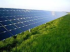
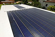
- Top: thin-film silicon laminates being installed onto a roof.
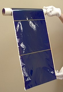
- Middle: CIGS solar cell on a flexible plastic backing and rigid CdTe panels mounted on a supporting structure
- Bottom: thin-film laminates on rooftops
Thin-film solar cells are made by depositing one or more thin layers (thin films or TFs) of photovoltaic material onto a substrate, such as glass, plastic or metal. Thin-film solar cells are typically a few nanometers (nm) to a few microns (μm) thick–much thinner than the wafers used in conventional crystalline silicon (c-Si) based solar cells, which can be up to 200 μm thick. Thin-film solar cells are commercially used in several technologies, including cadmium telluride (CdTe), copper indium gallium diselenide (CIGS), and amorphous thin-film silicon (a-Si, TF-Si).
Solar cells are often classified into so-called generations based on the active (sunlight-absorbing) layers used to produce them, with the most well-established or first-generation solar cells being made of single- or multi-crystalline silicon. This is the dominant technology currently used in most solar PV systems. Most thin-film solar cells are classified as second generation, made using thin layers of well-studied materials like amorphous silicon (a-Si), cadmium telluride (CdTe), copper indium gallium selenide (CIGS), or gallium arsenide (GaAs). Solar cells made with newer, less established materials are classified as third-generation or emerging solar cells. This includes some innovative thin-film technologies, such as perovskite, dye-sensitized, quantum dot, organic, and CZTS thin-film solar cells.
Thin-film cells have several advantages over first-generation silicon solar cells, including being lighter and more flexible due to their thin construction. This makes them suitable for use in building-integrated photovoltaics and as semi-transparent, photovoltaic glazing material that can be laminated onto windows. Other commercial applications use rigid thin film solar panels (interleaved between two panes of glass) in some of the world's largest photovoltaic power stations. Additionally, the materials used in thin-film solar cells are typically produced using simple and scalable methods more cost-effective than first-generation cells, leading to lower environmental impacts like greenhouse gas (GHG) emissions in many cases. Thin-film cells also typically outperform renewable and non-renewable sources for electricity generation in terms of human toxicity and heavy-metal emissions.
Despite initial challenges with efficient light conversion, especially among third-generation PV materials, as of 2023 some thin-film solar cells have reached efficiencies of up to 29.1% for single-junction thin-film GaAs cells, exceeding the maximum of 26.1% efficiency for standard single-junction first-generation solar cells. Multi-junction concentrator cells incorporating thin-film technologies have reached efficiencies of up to 47.6% as of 2023.[1]
Still, many thin-film technologies have been found to have shorter operational lifetimes and larger degradation rates than first-generation cells in accelerated life testing, which has contributed to their somewhat limited deployment. Globally, the PV marketshare of thin-film technologies remains around 5% as of 2023.[2] However, thin-film technology has become considerably more popular in the United States, where CdTe cells alone accounted for nearly 30% of new utility-scale deployment in 2022.[3]
History
Early research into thin-film solar cells began in the 1970s. In 1970, Zhores Alferov's team at Ioffe Institute created the first gallium arsenide (GaAs) solar cells, later winning the 2000 Nobel prize in Physics for this and other work.[4][5] Two years later in 1972, Prof. Karl Böer founded the Institute of Energy Conversion (IEC) at the University of Delaware to further thin-film solar research. The institute first focused on copper sulfide/cadmium sulfide (Cu2S/CdS) cells and later expanded to zinc phosphide (Zn3P2) and amorphous silicon (a-Si) thin-films as well in 1975.[6] In 1973, the IEC debuted a solar-powered house, Solar One, in the first example of residential building-integrated photovoltaics.[7] In the next decade, interest in thin-film technology for commercial use and aerospace[8] applications increased significantly, with several companies beginning development of amorphous silicon thin-film solar devices.[9] Thin-film solar efficiencies rose to 10% for Cu2S/CdS in 1980,[10] and in 1986 ARCO Solar launched the first commercially-available thin-film solar cell, the G-4000, made from amorphous silicon.[11]
In the 1990s and 2000s, thin-film solar cells saw significant increases in maximum efficiencies and expansion of existing thin-film technologies into new sectors. In 1992, a thin-film solar cell with greater than 15% efficiency was developed at University of South Florida.[12] Only seven years later in 1999, the U.S. National Renewable Energy Laboratory (NREL) and Spectrolab collaborated on a three-junction gallium arsenide solar cell that reached 32% efficiency.[13] That same year, Kiss + Cathcart designed transparent thin-film solar cells for some of the windows in 4 Times Square, generating enough electricity to power 5-7 houses.[14][12] In 2000, BP Solar introduced two new commercial solar cells based on thin-film technology.[12] In 2001, the first organic thin-film solar cells were developed at the Johannes Kepler University of Linz. In 2005, GaAs solar cells got even thinner with the first free-standing (no substrate) cells introduced by researchers at Radboud University.[15]
This was also a time of significant advances in the exploration of new third-generation solar materials–materials with the potential to overcome theoretical efficiency limits for traditional solid-state materials.[16] In 1991, the first high-efficiency dye-sensitized solar cell was developed, replacing the ordinary solid semiconducting (active) layer of the cell with a liquid electrolyte mixture containing light-absorbing dye.[17] In the early 2000s, development of quantum dot solar cells began,[16] technology later certified by NREL in 2011.[18] In 2009, researchers at the University of Tokyo reported a new type solar cell using perovskites as the active layer and achieving over 3% efficiency,[19] building on Murase Chikao's 1999 work which created a perovskite layer capable of absorbing light.[20]
In the 2010s and early 2020s, innovation in thin-film solar technology has included efforts to expand third-generation solar technology to new applications and to decrease production costs, as well as significant efficiency improvements for both second and third generation materials. In 2015, Kyung-In Synthetic released the first inkjet solar cells, flexible solar cells made with industrial printers.[21] In 2016, Vladimir Bulović's Organic and Nanostructured Electronics (ONE) Lab at the Massachusetts Institute of Technology (MIT) created thin-film cells light enough to sit on top of soap bubbles.[22] In 2022, the same group introduced flexible organic thin-film solar cells integrated into fabric.[23][24]
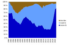
Thin-film solar technology captured a peak global market share of 32% of the new photovoltaic deployment in 1988 before declining for several decades and reaching another, smaller peak of 17% again in 2009.[25][26] Market share then steadily declined to 5% in 2021 globally,[25] however thin-film technology captured approximately 19% of the total U.S. market share in the same year, including 30% of utility-scale production.[27]
Theory of operation
In a typical solar cell, the photovoltaic effect is used to generate electricity from sunlight. The light-absorbing or "active layer" of the solar cell is typically a semiconducting material, meaning that there is a gap in its energy spectrum between the valence band of localized electrons around host ions and the conduction band of higher-energy electrons which are free to move throughout the material. For most semiconducting materials at room temperature, electrons which have not gained extra energy from another source will exist largely in the valence band, with few or no electrons in the conduction band. When a solar photon reaches the semiconducting active layer in a solar cell, electrons in the valence band can absorb the energy of the photon and be excited into the conduction band, allowing them to move freely throughout the material. When this happens, an empty electron state (or hole) is left behind in the valence band. Together, the conduction band electron and the valence band hole are called an electron-hole pair. Both the electron and the hole in the electron-hole pair can move freely throughout the material as electricity.[28] However, if the electron-hole pair is not separated, the electron and hole can recombine into the lower-energy original state, releasing a photon of the corresponding energy. In thermodynamic equilibrium, the forward process (absorbing a photon to excite an electron-hole pair) and reverse process (emitting a photon to destroy an electron-hole pair) must occur at the same rate by the principle of detailed balance. Therefore, to construct a solar cell from a semiconducting material and extract current during the excitation process, the electron and hole of the electron-hole pair must be separated. This can be achieved in a variety of different ways, but the most common is with a p-n junction, where a positively doped (p-type) semiconducting layer and a negatively doped (n-type) semiconducting layer meet, creating a chemical potential difference which draws electrons one direction and holes the other, separating the electron-hole pair.[29] This may instead be achieved using metal contacts with different work functions, as in a Schottky-junction cell.
In a thin-film solar cell, the process is largely the same but the active semiconducting layer is made much thinner. This may be made possible by some intrinsic property of the semiconducting material used that allows it to convert a particularly large number of photons per thickness. For example, some thin-film materials having a direct bandgap, meaning the conduction and valence band electron states are at the same momentum instead of different momenta as in the case of an indirect bandgap semiconductor like silicon. Having a direct bandgap eliminates the need for a source or sink of momentum (typically a lattice vibration, or phonon), simplifying the two-step process of absorbing a photon into a single-step process.[30] Other thin-film materials may be able to absorb more photons per thickness simply due to having an energy bandgap that is well-matched to the peak energy of the solar spectrum, meaning there are many solar photons of the correct energy available to excite electron-hole pairs.
In other thin-film solar cells, the semiconducting layer may be replaced entirely with another light-absorbing material, for example an electrolyte solution and photo-active dye molecules in a dye-sensitized solar cell or by quantum dots in a quantum dot solar cell.
Materials
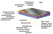
Thin-film technologies reduce the amount of active material in a cell. The active layer may be placed on a rigid substrate made from glass, plastic, or metal or the cell may be made with a flexible substrate like cloth. Thin-film solar cells tend to be cheaper than crystalline silicon cells and have a smaller ecological impact (determined from life cycle analysis).[31] Their thin and flexible nature also makes them ideal for applications like building-integrated photovoltaics. The majority of film panels have 2-3 percentage points lower conversion efficiencies than crystalline silicon,[32] though some thin-film materials outperform crystalline silicon panels in terms of efficiency. Cadmium telluride (CdTe), copper indium gallium selenide (CIGS) and amorphous silicon (a-Si) are three of the most prominent thin-film technologies.
Second-generation thin-film materials
Cadmium telluride
Cadmium telluride (CdTe) is a chalcogenide material that is the predominant thin film technology. With about 5 percent of worldwide PV production, it accounts for more than half of the thin film market. The cell's lab efficiency has also increased significantly in recent years and is on a par with CIGS thin film and close to the efficiency of multi-crystalline silicon as of 2013.[33]: 24–25 Also, CdTe has the lowest energy payback time of all mass-produced PV technologies, and can be as short as eight months in favorable locations.[33]: 31 CdTe also performs better than most other thin-film PV materials across many important environmental impact factors like global warming potential and heavy metal emissions.[34] A prominent manufacturer is the US-company First Solar based in Tempe, Arizona, that produces CdTe-panels with an efficiency of about 18 percent.[35]
Although the toxicity of cadmium may not be that much of an issue and environmental concerns completely resolved with the recycling of CdTe modules at the end of their life time,[36] there are still uncertainties[37] and the public opinion is skeptical towards this technology.[38][39] The usage of rare materials may also become a limiting factor to the industrial scalability of CdTe thin film technology. The rarity of tellurium—of which telluride is the anionic form—is comparable to that of platinum in the earth's crust and contributes significantly to the module's cost.[40]
Copper indium gallium selenide (CIGS)
| Cell | Module | |
| Glass substrate | 23.6 %[41] | 20.3 %[42] |
| Flexible substrate | 22.2 %[43] | 18.6 %[44] |
Like CdTe, copper indium gallium selenide (CIGS) and its variations are chalcogenide compound semiconductors. CIGS solar cells reached a lab-efficiency above 23 percent (see table) and a share of 0.8 percent in the overall PV market in 2021.[45] Numerous companies have produced CIGS solar cells and modules, however, some of them have significantly reduced or ceased production during the last years.
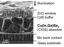
Actual research aims at improving properties related to fabrication and functionality by modifying or replacing the individual layers, for example:
- Alternative materials are investigated to replace cadmium sulfide as a buffer layer due to its hazard potential.[46]
- Molybdenum as a back contact is replaced by a transparent conducting film in order to obtain bifacial solar cells.[47]

- CIGS solar cells show a particularly low loss in efficiency, when deposited on a flexible substrate instead of glass (see table), hence they are considered promising candidates for bendable and lightweight solar modules.[48]
Apart from the development potential of the other layers in the solar cell, the absorber material CIGS has the remarkable property, that its band gap can be tuned by adjusting the ratio of indium and gallium in the compound. By tuning the band gap, the fraction of the solar spectrum which is absorbed by the solar cell can be changed, making CIGS cells especially interesting as constituents of multi-junction solar cells.[48]
It is also possible to partially replace copper by silver and selenium by sulfur yielding the compound (AgzCu1-z)(In1-xGax)(Se1-ySy)2. In order to distinguish the sulfur-free compound, it is sometimes abbrievated CIGSe, while the acronym CIGS can refer to both sulfur and selenium containing compounds. The silver containing compound is sometimes referred to as ACIGS. Variations of the CIGS composition are subject to current research and in part also fabricated in industry.
Silicon
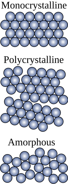
There are three prominent silicon thin-film architectures:
- Amorphous silicon cells
- Amorphous / microcrystalline tandem cells (micromorph)
- Thin-film polycrystalline silicon on glass.[49]
Amorphous silicon
Amorphous silicon (a-Si) is a non-crystalline, allotropic form of silicon and the most well-developed thin film technology to-date. Thin-film silicon is an alternative to conventional wafer (or bulk) crystalline silicon. While chalcogenide-based CdTe and CIS thin films cells have been developed in the lab with great success, there is still industry interest in silicon-based thin film cells. Silicon-based devices exhibit fewer problems than their CdTe and CIS counterparts such as toxicity and humidity issues with CdTe cells and low manufacturing yields of CIS due to material complexity. Additionally, due to political resistance to the use non-"green" materials in solar energy production, there is no stigma in the use of standard silicon.
This type of thin-film cell is mostly fabricated by a technique called plasma-enhanced chemical vapor deposition. It uses a gaseous mixture of silane (SiH4) and hydrogen to deposit a very thin layer of only 1 micrometre (μm) of silicon on a substrate, such as glass, plastic or metal, that has already been coated with a layer of transparent conducting oxide. Other methods used to deposit amorphous silicon on a substrate include sputtering and hot wire chemical vapor deposition techniques.[50]
a-Si is attractive as a solar cell material because it's an abundant, non-toxic material. It requires a low processing temperature and enables a scalable production upon a flexible, low-cost substrate with little silicon material required. Due to its bandgap of 1.7 eV, amorphous silicon also absorbs a very broad range of the light spectrum, that includes infrared and even some ultraviolet and performs very well at weak light. This allows the cell to generate power in the early morning, or late afternoon and on cloudy and rainy days, contrary to crystalline silicon cells, that are significantly less efficient when exposed at diffuse and indirect daylight.[citation needed]
However, the efficiency of an a-Si cell suffers a significant drop of about 10 to 30 percent during the first six months of operation. This is called the Staebler-Wronski effect (SWE) – a typical loss in electrical output due to changes in photoconductivity and dark conductivity caused by prolonged exposure to sunlight. Although this degradation is perfectly reversible upon annealing at or above 150 °C, conventional c-Si solar cells do not exhibit this effect in the first place.
Its basic electronic structure is the p-i-n junction. The amorphous structure of a-Si implies high inherent disorder and dangling bonds, making it a bad conductor for charge carriers. These dangling bonds act as recombination centers that severely reduce carrier lifetime. A p-i-n structure is usually used, as opposed to an n-i-p structure. This is because the mobility of electrons in a-Si:H is roughly 1 or 2 orders of magnitude larger than that of holes, and thus the collection rate of electrons moving from the n- to p-type contact is better than holes moving from p- to n-type contact. Therefore, the p-type layer should be placed at the top where the light intensity is stronger, so that the majority of the charge carriers crossing the junction are electrons.[51]
Tandem-cell using a-Si/μc-Si
A layer of amorphous silicon can be combined with layers of other allotropic forms of silicon to produce a multi-junction solar cell. When only two layers (two p-n junctions) are combined, it is called a tandem-cell. By stacking these layers on top of one other, a broader range of the light spectra is absorbed, improving the cell's overall efficiency.
In micromorphous silicon, a layer of microcrystalline silicon (μc-Si) is combined with amorphous silicon, creating a tandem cell. The top a-Si layer absorbs the visible light, leaving the infrared part to the bottom μc-Si layer. The micromorph stacked-cell concept was pioneered and patented at the Institute of Microtechnology (IMT) of the Neuchâtel University in Switzerland,[52] and was licensed to TEL Solar. A new world record PV module based on the micromorph concept with 12.24% module efficiency was independently certified in July 2014.[53]
Because all layers are made of silicon, they can be manufactured using PECVD. The band gap of a-Si is 1.7 eV and that of c-Si is 1.1 eV. The c-Si layer can absorb red and infrared light. The best efficiency can be achieved at transition between a-Si and c-Si. As nanocrystalline silicon (nc-Si) has about the same bandgap as c-Si, nc-Si can replace c-Si.[54]

Tandem-cell using a-Si/pc-Si
Amorphous silicon can also be combined with protocrystalline silicon (pc-Si) into a tandem-cell. Protocrystalline silicon with a low volume fraction of nanocrystalline silicon is optimal for high open-circuit voltage.[55] These types of silicon present dangling and twisted bonds, which results in deep defects (energy levels in the bandgap) as well as deformation of the valence and conduction bands (band tails).
Polycrystalline silicon on glass
A new attempt to fuse the advantages of bulk silicon with those of thin-film devices is thin film polycrystalline silicon on glass. These modules are produced by depositing an antireflection coating and doped silicon onto textured glass substrates using plasma-enhanced chemical vapor deposition (PECVD). The texture in the glass enhances the efficiency of the cell by approximately 3% by reducing the amount of incident light reflecting from the solar cell and trapping light inside the solar cell. The silicon film is crystallized by an annealing step, temperatures of 400–600 Celsius, resulting in polycrystalline silicon.
These new devices show energy conversion efficiencies of 8% and high manufacturing yields of >90%. Crystalline silicon on glass (CSG), where the polycrystalline silicon is 1–2 micrometres, is noted for its stability and durability; the use of thin film techniques also contributes to a cost savings over bulk photovoltaics. These modules do not require the presence of a transparent conducting oxide layer. This simplifies the production process twofold; not only can this step be skipped, but the absence of this layer makes the process of constructing a contact scheme much simpler. Both of these simplifications further reduce the cost of production. Despite the numerous advantages over alternative design, production cost estimations on a per unit area basis show that these devices are comparable in cost to single-junction amorphous thin film cells.[49]
Gallium arsenide
Gallium arsenide (GaAs) is a III-V direct bandgap semiconductor and is a very common material used for single-crystalline thin-film solar cells. GaAs solar cells have continued to be one of the highest performing thin-film solar cells due to their exceptional heat resistant properties and high efficiencies.[56] As of 2019, single-crystalline GaAs cells have shown the highest solar cell efficiency of any single-junction solar cell with an efficiency of 29.1%.[57] This record-holding cell achieved this high efficiency by implementing a back mirror on the rear surface to increase photon absorption which allowed the cell to attain an impressive short-circuit current density and an open-circuit voltage value near the Shockley–Queisser limit.[58] As a result, GaAs solar cells have nearly reached their maximum efficiency although improvements can still be made by employing light trapping strategies.[59]
GaAs thin-films are most commonly fabricated using epitaxial growth of the semiconductor on a substrate material. The epitaxial lift-off (ELO) technique, first demonstrated in 1978, has proven to be the most promising and effective. In this method, the thin film layer is peeled off of the substrate by selectively etching a sacrificial layer that was placed between the epitaxial film and substrate.[60] The GaAs film and the substrate remain minimally damaged through the separation process, allowing for the reuse of the host substrate.[61] With reuse of the substrate the fabrication costs can be reduced, but not completely forgone, since the substrate can only be reused a limited number of times.[59] This process is still relatively costly and research is still being done to find more cost-effective ways of growing the epitaxial film layer onto a substrate.
Despite the high performance of GaAs thin-film cells, the expensive material costs hinder their ability for wide-scale adoption in the solar cell industry. GaAs is more commonly used in multi-junction solar cells for solar panels on spacecraft, as the larger power to weight ratio lowers the launch costs in space-based solar power (InGaP/(In)GaAs/Ge cells). They are also used in concentrator photovoltaics, an emerging technology best suited for locations that receive much sunlight, using lenses to focus sunlight on a much smaller, thus less expensive GaAs concentrator solar cell.
Third-generation (emerging) thin-film materials
The National Renewable Energy Laboratory classifies a number of thin-film technologies as emerging photovoltaics—most of them have not yet been commercially applied and are still in the research or development phase. Many use organic materials, often organometallic compounds as well as inorganic substances. Though many of these technologies have struggled with instability and low efficiencies in their early stages, some emerging materials like perovskites have been able to attain efficiencies comparable to mono crystalline silicon cells. Many of these technologies have the potential to beat the Shockley–Queisser limit for efficiency of a single-junction solid-state cell. Significant research has been invested into these technologies as they promise to achieve the goal of producing low-cost, high-efficiency solar cells with smaller environmental impacts.
Copper zinc tin sulfide (CZTS)
Copper zinc tin sulfide or Cu(Zn,Sn)(S,Se)2, commonly abbreviated CZTS, and its derivatives CZTSe and CZTSSe belong to a group chalcogenides (like CdTe and CIGS/CIS) sometimes called kesterites. Unlike CdTe and CIGS, CZTS is made from abundant and non-toxic raw materials. Additionally, the bandgap of CZTS can be tuned by changing the S/Se ratio, which is a desirable property for engineering of optimal solar cells.[62] CZTS also has a high light absorption coefficient.
Other emerging chalcogenide PV materials include antimony-based compounds like Sb2(S,Se)3. Like CZTS, they have tunable bandgaps and good light absorption. Antimony-based compounds also have a quasi-1D structure which may be useful for device engineering. All of these emerging chalcogenide materials have the advantage of being a part of one of the most mature and efficient families of thin-film technology. As of 2022, CZTS cells have achieved a maximum efficiency of around 12.6% while antimony-based cells have reached 9.9%.[63]
Dye-sensitized (DSPV)
Dye-sensitized cells, also known as Grätzel cells or DSPV, are innovative cells that perform a kind of artificial photosynthesis,[64] removing the need for a bulk solid-state semiconductor or a p-n junction. Instead, they are constructed using a layer of photoactive dye mixed with semiconductor transition metal oxide nanoparticles on top of a liquid electrolyte solution, surrounded by electrical contacts made of platinum or sometimes graphene and encapsulated in glass. When photons enter the cell, they can be absorbed by the dye molecules, putting them into their sensitized state. In this state, the dye molecules can inject electrons into the semiconductor conduction band. The dye electrons are then replenished by the electrode, preventing recombination of the electron-hole pair. The electron in the semiconductor flows out as current through the electrical contacts.[65]
Dye-sensitized solar cells are attractive because they allow for cheap and cost-efficient roll-based manufacturing.[62] In practice, however, the inclusion of expensive materials like platinum and ruthenium keep these low costs from being achieved.[62] Dye-sensitized cells also have issues with stability and degradation, particularly because of the liquid electrolyte. In high temperature environments, the electrolyte may leak from the cell while in low temperature environments the electrolyte may freeze. Some of these issues can be overcome using a quasi-solid state electrolyte.[64]
As of 2023, the maximum realized efficiency of a dye-sensitized solar cell is around 13%.[66]
Organic photovoltaics (OPV)
Organic solar cells use organic semiconducting polymers as the photoactive material. These organic polymers are cost-effective to produce and are tunable with high absorption coefficients.[64] Organic solar cell manufacturing is also cost effective and can make use of efficient roll-to-roll production techniques. They also have some of the lowest environmental impact scores of all PV technologies across a wide range of impact factors including energy payback time global warming potential.[67]
Organic cells and are naturally flexible, lending themselves well to many applications. Scientists at the Massachusetts Institute of Technology (MIT)'s Organic and Nanostructured Electronics Lab (ONE Lab) have integrated organic PV onto flexible fabric substrates that can be unrolled over 500 times without degradation.[23]
However, organic solar cells are generally not very stable and tend to have low operational lifetimes. They also tend to be less efficient than other thin-film cells due to some intrinsic limits of the material like a large binding energy for electron-hole pairs.[64] As of 2023, the maximum achieved efficiency for organic solar cells is 18.2%.[66]
Perovskite solar cells
Perovskites are a group of materials with a shared crystal structure, named after their discoverer, mineralogist Lev Perovski. The perovskites most often used for PV applications are organic-inorganic hybrid methylammonium lead halides, which host a number of advantageous properties including widely tunable bandgaps, high absorption coefficients, and good electronic transport properties for both electrons and holes.[68] As of 2023, single-junction perovskite solar cells achieved a maximum efficiency of 25.7%, rivaling that of mono crystalline silicon. Perovskites are also commonly used in tandem and multi-junction cells with crystalline silicon, CIGS, and other PV technologies to achieve even higher efficiencies.[66] They also offer a wide spectrum of low-cost applications.[69][70][71]
However, perovskite cells tend to have short lifetimes, with 5 years being a typical lifetime as of 2016.[68] This is mostly due to their chemical instability when exposed to light, moisture, UV radiation, and high temperatures which may even cause them to undergo a structural transition that impacts the operation of the device. Therefore, proper encapsulation is very important.[64]
Quantum dot photovoltaics (QDPV)
Quantum dot photovoltaics (QDPV) replace the usual solid-state semiconducting active layer with semiconductor quantum dots. The bandgap of the photo-active layer can be tuned by changing the size of the quantum dots.[62] QDPV has the potential to generate more than one electron-hole pair per photon in a process called multiple exciton generation (MEG) which could allow for a theoretical maximum conversion efficiency of 87%,[34] though as of 2023 the maximum achieved efficiency of a QDPV cell is around 18.1%.[66] QDPV cells also tend to use much less of the active layer material than other solar cell types leading to a low-cost manufacturing process. However, QDPV cells tend to have high environmental impacts compared to other thin-film PV materials, especially human toxicity and heavy metal emissions.[34]
Applications
Transparent solar cells
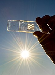
In 2022, semitransparent solar cells that are as large as windows were reported,[72] after team members of the study achieved record efficiency with high transparency in 2020.[73][74] Also in 2022, other researchers reported the fabrication of solar cells with a record average visible transparency of 79%, being nearly invisible.[75][76]
Building-integrated photovoltaics
Thin-film PV materials tend to be lightweight and flexible in nature, which lends itself naturally to building-integrated photovoltaics (BIPV).[77] Common examples include the integration of semi-transparent modules can be integrated into window designs[78] and the use of rigid thin-film panels to replace roofing material. BIPV can greatly reduce the lifetime environmental impacts (like greenhouse gas (GHG) emission) due to solar cell modules due to the avoided emissions associated with not utilizing the usual building materials.[79]
Efficiencies
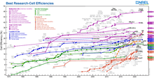
Despite initially lower efficiencies at the time of their introduction, many thin-film technologies have efficiencies comparable to conventional single-junction non-concentrator crystalline silicon solar cells which have a 26.1% maximum efficiency as of 2023. Im fact, both GaAs thin-film and GaAs single-crystal cells have larger maximum efficiencies of 29.1% and 27.4% respectively. The maximum efficiencies for single-junction non-concentrator thin-film cells of various prominent thin-film materials are shown in the chart.
| Solar Cell Type | Best Efficiency (%) | ||||||||
|---|---|---|---|---|---|---|---|---|---|
| GaAs thin-film | 29.1
| ||||||||
| GaAs single crystal | 27.8
| ||||||||
| Single-crystal silicon* | 26.1
| ||||||||
| Perovskites | 25.7
| ||||||||
| Multi-crystalline silicon* | 24.4
| ||||||||
| CIGS | 23.6
| ||||||||
| CdTe | 22.1
| ||||||||
| Thin-film c-Si | 21.7
| ||||||||
| Organic | 18.2
| ||||||||
| Quantum dot | 18.1
| ||||||||
| Amorphous silicon | 14
| ||||||||
| Dye-sensitized | 13
| ||||||||
| CZTSSe | 13
| ||||||||
|
*Not thin-film, included for comparison only. Data from NREL 2023 Best Research-Cell Efficiency dataset. | |||||||||
Commercial module efficiences
It's important to note that the maximum efficiencies achieved in a laboratory setting are generally higher than the efficiencies of manufactured cells, which often have efficiencies 20-50% lower.[68] As of 2021, the maximum efficiency of manufactured solar cells was 24.4% for mono crystalline silicon, 20.4% for poly crystalline silicon, 12.3% for amorphous silicon, 19.2% for CIGS, and 19% for CdTe modules.[80] The thin film cell prototype with the best efficiency yields 20.4% (First Solar), comparable to the best conventional solar cell prototype efficiency of 25.6% from Panasonic.[81][82]
A previous record for thin film solar cell efficiency of 22.3% was achieved by Solar Frontier, the world's largest CIS (copper indium selenium) solar energy provider. In joint research with the New Energy and Industrial Technology Development Organization (NEDO) of Japan, Solar Frontier achieved 22.3% conversion efficiency on a 0.5 cm2 cell using its CIS technology. This was an increase of 0.6 percentage points over the industry's previous thin-film record of 21.7%.[83]
Calculation of efficiency
The efficiency of a solar cell quantifies the percentage of incident light on the solar cell that is converted into usable electricity. There are many factors that affect the efficiency of a solar cell, so the efficiency may be further parametrized by additional numerical quantities including the short-circuit current, open-circuit voltage, maximum power point, fill factor, and quantum efficiency. The short-circuit current is the maximum current the cell can flow with no voltage load. Similarly, the open-circuit voltage is the voltage across the device with no current or, alternatively, the voltage required for no current to flow. On a current vs. voltage (IV) curve, the open-circuit voltage is the horizontal intercept of the curve with the voltage axis and the short-circuit current is the vertical intercept of the curve with the current axis. The maximum power point is the point along the curve where the maximum power output of the solar cell is achieved and the area of the rectangle with side lengths equal to the current and voltage coordinates of the maximum power point is called the fill factor. The fill factor is a measure of how much power the solar cell achieves at this maximum power point. Intuitively, IV curves with a more square shape and a flatter top and side will have a larger fill factor and therefore a higher efficiency.[84] Whereas these parameters characterize the efficiency of the solar cell based mostly on its macroscopic electrical properties, the quantum efficiency measures either the ratio of the number of photons incident on the cell to the number of charge carriers extracted (external quantum efficiency) or the ratio of the number of photons absorbed by the cell to the number of charge carriers extracted (internal quantum efficiency). Either way, the quantum efficiency is a more direct probe of the microscopic structure of the solar cell.[85]

Increasing efficiencyedit
Some third-generation solar cells boost efficiency through the integration of concentrator and/or multi-junction device geometry.[63] This can lead to efficiencies larger than the Shockley–Queisser limit of approximately 42% efficiency for a single-junction semiconductor solar cell under one-sun illumination.[86]
A multi-junction cell is one that incorporates multiple semiconducting active layers with different bandgaps. In a typical solar cell, a single absorber with a bandgap near the peak of the solar spectrum is used, and any photons with energy greater than or equal to the bandgap can excite valence-band electrons into the conduction band to create electron-hole pairs. However, any excess energy above the Fermi energy will be quickly dissipated due to thermalization, leading to voltage losses from the inability to efficiently extract the energy of high-energy photons. Mutli-junction cells are able to recoup some of this energy lost to thermalization by stacking multiple absorber layers on top of each other with the top layer absorbing the highest-energy photons and letting the lower energy photons pass through to the lower layers with smaller bandgaps, and so on. This not only allows the cells to capture energy from photons in a larger range of energies, but also extracts more energy per photon from the higher-energy photons.[citation needed]
Concentrator photovoltaics use an optical system of lenses that sit on top of the cell to focus light from a larger area onto the device, similar to a funnel for sunlight. In addition to creating more electron-hole pairs simply by increasing the number of photons available for absorption, having a higher concentration of charge carriers can increase the efficiency of the solar cell by increasing the conductivity. The addition of a concentrator to a solar cell can not only increase efficiency, but can also reduce the space, materials, and cost needed to produce the cell.[87]
Both of these techniques are employed in the highest-efficiency solar cell as of 2023, which is a four-junction concentrator cell with 47.6% efficiency.[1]
| Solar Cell Type | Best Efficiency (%) |
|---|---|
| 4+ junction concentrator | 47.6(GaInP/AlGaAs/GaInAsP/GaInAs)
|
| 3-junction concentrator | 44.4(GaInP/GaAs/GaInAs)
|
| 3-junction non-concentrator | 39.46(GaInP/mQW-GaAs/GaInAs)
|
| 4+ junction non-concentrator | 39.2(AlGaInP/AlGaAs/GaAs/GaInAs)
|
| 2-junction concentrator | 35.5(GaInAsP/GaInAs)
|
| 2-junction non-concentrator | 32.9(GaInP/GaAs)
|
| Perovskite/Si tandem | 32.5
|
| GaAs concentrator | 30.8
|
| Si single-crystal concentrator | 27.6
|
| Si HIT | 26.81
|
| Perovskite/CIGS tandem | 24.2
|
| CIGS concentrator | 23.3
|
| Organic tandem | 14.2(PDTB-EF-T/IT-4F)
|


