

A | B | C | D | E | F | G | H | CH | I | J | K | L | M | N | O | P | Q | R | S | T | U | V | W | X | Y | Z | 0 | 1 | 2 | 3 | 4 | 5 | 6 | 7 | 8 | 9
 | |
| General information | |
|---|---|
| Launched | 1975 |
| Common manufacturer | |
| Performance | |
| Max. CPU clock rate | 1 MHz to 3 MHz |
| Data width | 8 bits |
| Address width | 16 bits |
| Architecture and classification | |
| Instruction set | MOS 6502 |
| Number of instructions | 56 (55 originally) |
| Physical specifications | |
| Transistors | |
| Package |
|
| History | |
| Predecessors |
|
| Successors | |
The MOS Technology 6502 (typically pronounced "sixty-five-oh-two")[3] is an 8-bit microprocessor that was designed by a small team led by Chuck Peddle for MOS Technology. The design team had formerly worked at Motorola on the Motorola 6800 project; the 6502 is essentially a simplified, less expensive and faster version of that design.
When it was introduced in 1975, the 6502 was the least expensive microprocessor on the market by a considerable margin. It initially sold for less than one-sixth the cost of competing designs from larger companies, such as the 6800 or Intel 8080. Its introduction caused rapid decreases in pricing across the entire processor market. Along with the Zilog Z80, it sparked a series of projects that resulted in the home computer revolution of the early 1980s.
Popular video game consoles and home computers of the 1980s and early 1990s, such as the Atari 2600, Atari 8-bit computers, Apple II, Nintendo Entertainment System, Commodore 64, Atari Lynx, BBC Micro and others, use the 6502 or variations of the basic design. Soon after the 6502's introduction, MOS Technology was purchased outright by Commodore International, who continued to sell the microprocessor and licenses to other manufacturers. In the early days of the 6502, it was second-sourced by Rockwell and Synertek, and later licensed to other companies.
In 1981, the Western Design Center started development of a CMOS version, the 65C02. This continues to be widely used in embedded systems, with estimated production volumes in the hundreds of millions.[4]
History and use
Origins at Motorola

The 6502 was designed by many of the same engineers that had designed the Motorola 6800 microprocessor family.[5] Motorola started the 6800 microprocessor project in 1971 with Tom Bennett as the main architect. Motorola's engineers could run analog and digital simulations on an IBM 370-165 mainframe computer.[6] The chip layout began in late 1972, the first 6800 chips were fabricated in February 1974 and the full family was officially released in November 1974.[7][8]
John Buchanan was the designer of the 6800 chip[9][10] and Rod Orgill, who later did the 6501, assisted Buchanan with circuit analyses and chip layout.[11] Bill Mensch joined Motorola in June 1971 after graduating from the University of Arizona (at age 26).[12] His first assignment was helping define the peripheral ICs for the 6800 family and later he was the principal designer of the 6820 Peripheral Interface Adapter (PIA).[13] Bennett hired Chuck Peddle in 1973 to do architectural support work on the 6800 family products already in progress.[14] He contributed in many areas, including the design of the 6850 ACIA (serial interface).[15]
Motorola's target customers were established electronics companies such as Hewlett-Packard, Tektronix, TRW, and Chrysler.[16] In May 1972, Motorola's engineers began visiting select customers and sharing the details of their proposed 8-bit microprocessor system with ROM, RAM, parallel and serial interfaces.[17] In early 1974, they provided engineering samples of the chips so that customers could prototype their designs. Motorola's "total product family" strategy did not focus on the price of the microprocessor, but on reducing the customer's total design cost. They offered development software on a timeshare computer, the "EXORciser" debugging system, onsite training and field application engineer support.[18][19] Both Intel and Motorola had initially announced a US$360 price for a single microprocessor.[20][21] The actual price for production quantities was much less. Motorola offered a design kit containing the 6800 with six support chips for US$300.[22]
Peddle, who would accompany the salespeople on customer visits, found that customers were put off by the high cost of the microprocessor chips.[23] At the same time, these visits invariably resulted in the engineers he presented to producing lists of required instructions that were much smaller than "all these fancy instructions" that had been included in the 6800.[24] Peddle and other team members started outlining the design of an improved feature, reduced size microprocessor. At that time, Motorola's new semiconductor fabrication facility in Austin, Texas, was having difficulty producing MOS chips, and mid-1974 was the beginning of a year-long recession in the semiconductor industry. Also, many of the Mesa, Arizona employees were displeased with the upcoming relocation to Austin.[25]
Motorola's Semiconductor Products Division management showed no interest in Peddle's low-cost microprocessor proposal. Eventually Peddle was given an official letter telling him to stop working on the system.[26] Peddle responded to the order by informing Motorola that the letter represented an official declaration of "project abandonment", and as such, the intellectual property he had developed to that point was now his.[27] In a November 1975 interview, Motorola's Chairman, Robert Galvin, ultimately agreed that Peddle's concept was a good one and that the division missed an opportunity, "We did not choose the right leaders in the Semiconductor Products division." The division was reorganized and the management replaced. The new group vice-president John Welty said, "The semiconductor sales organization lost its sensitivity to customer needs and couldn't make speedy decisions."[28]
MOS Technology


Peddle began looking outside Motorola for a source of funding for this new project. He initially approached Mostek CEO L. J. Sevin, but was declined. Sevin later admitted this was because he was afraid Motorola would sue them.[29]
While Peddle was visiting Ford Motor Company on one of his sales trips, Bob Johnson, later head of Ford's engine automation division, mentioned that their former colleague John Paivinen had moved to General Instrument and taught himself semiconductor design.[30] Paivinen then formed MOS Technology in Valley Forge, Pennsylvania in 1969 with two other executives from General Instrument, Mort Jaffe and Don McLaughlin. Allen-Bradley, a supplier of electronic components and industrial controls, acquired a majority interest in 1970.[31] The company designed and fabricated custom ICs for customers and had developed a line of calculator chips.[32]
After the Mostek efforts fell through, Peddle approached Paivinen, who "immediately got it".[33] On 19 August 1974, Chuck Peddle, Bill Mensch, Rod Orgill, Harry Bawcom, Ray Hirt, Terry Holdt, and Wil Mathys left Motorola to join MOS. Mike Janes joined later. Of the seventeen chip designers and layout people on the 6800 team, eight left. The goal of the team was to design and produce a low-cost microprocessor for embedded applications and to target as wide as possible a customer base. This would be possible only if the microprocessor was low cost, and the team set the price goal for volume purchases at $5.[34] Mensch later stated the goal was not the processor price itself, but to create a set of chips that could sell at $20 to compete with the recently introduced Intel 4040 that sold for $29 in a similar complete chipset.[35]
Chips are produced by printing multiple copies of the chip design on the surface of a "wafer", a thin disk of highly pure silicon. Smaller chips can be printed in greater numbers on the same wafer, decreasing their relative price. Additionally, wafers always include some number of tiny physical defects that are scattered across the surface. Any chip printed in that location will fail and has to be discarded. Smaller chips mean any single copy is less likely to be printed on a defect. For both of these reasons, the cost of the final product is strongly dependent on the size of the chip design.[36]
The original 6800 chips were intended to be 180 by 180 mils (4.6 mm × 4.6 mm), but layout was completed at 212 by 212 mils (5.4 mm × 5.4 mm), or an area of 29.0 mm2.[37] For the new design, the cost goal demanded a size goal of 153 by 168 mils (3.9 mm × 4.3 mm), or an area of 16.6 mm2.[38] Several new techniques would be needed to hit this goal.
Moving to NMOS
There were two significant advances that arrived in the market just as the 6502 was being designed that provided significant cost reductions. The first was the move to depletion-load NMOS. The 6800 used an early NMOS process, enhancement mode, that required three supply voltages. One of the 6800's headlining features was an onboard voltage doubler that allowed a single +5 V supply be used for +5, −5 and +12 V internally, as opposed to other chips of the era like the Intel 8080 that required three separate supply pins.[39] While this feature reduced the complexity of the power supply and pin layout, it still required separate power line to the various gates on the chip, driving up complexity and size. By moving to the new depletion-load design, a single +5 V supply was all that was needed, eliminating all of this complexity.[40]
A further advantage was that depletion-load designs used less power while switching, thus running cooler and allowing higher operating speeds. Another practical offshoot is that the clock signal for earlier CPUs had to be strong enough to survive all the dissipation as it traveled through the circuits, which almost always required a separate external chip that could supply a powerful signal. With the reduced power requirements of depletion-load, the clock could be moved onto the chip, simplifying the overall computer design. These changes greatly reduced complexity and the cost of implementing a complete system.[40]
A wider change taking place in the industry was the introduction of projection masking. Previously, chips were patterned onto the surface of the wafer by placing a mask on the surface of the wafer and then shining a bright light on it. The masks often picked up tiny bits of dirt or photoresist as they were lifted off the chip, causing flaws in those locations on any subsequent masking. With complex designs like CPUs, 5 or 6 such masking steps would be used, and the chance that at least one of these steps would introduce a flaw was very high. In most cases, 90% of such designs were flawed, resulting in a 10% yield. The price of the working examples had to cover the production cost of the 90% that were thrown away.[41]
In 1973, Perkin-Elmer introduced the Micralign system, which projected an image of the mask on the wafer instead of requiring direct contact. Masks no longer picked up dirt from the wafers and lasted on the order of 100,000 uses rather than 10. This eliminated step-to-step failures and the high flaw rates formerly seen on complex designs. Yields on CPUs immediately jumped from 10% to 60 or 70%. This meant the price of the CPU declined roughly the same amount and the microprocessor suddenly became a commodity device.[41]
MOS Technology's existing fabrication lines were based on the older PMOS technology, they had not yet begun to work with NMOS when the team arrived. Paivinen promised to have an NMOS line up and running in time to begin the production of the new CPU. He delivered on the promise, the new line was ready by June 1975.[42]
Design notes
Chuck Peddle, Rod Orgill, and Wil Mathys designed the initial architecture of the new processors. A September 1975 article in EDN magazine gives this summary of the design:[43]
The MOS Technology 650X family represents a conscious attempt of eight former Motorola employees who worked on the development of the 6800 system to put out a part that would replace and outperform the 6800, yet undersell it. With the benefit of hindsight gained on the 6800 project, the MOS Technology team headed by Chuck Peddle, made the following architectural changes in the Motorola CPU…
The main change in terms of chip size was the elimination of the tri-state drivers from the address bus outputs. A three-state bus has states for "1", "0" and "high impedance". The last state is used to allow other devices to access the bus, and is typically used for multiprocessing, or more commonly in these roles, for direct memory access (DMA). While useful, this feature is very expensive in terms of on-chip circuitry. The 6502 simply removed this feature, in keeping with its design as an inexpensive controller being used for specific tasks and communicating with simple devices. Peddle suggested that anyone that actually required this style of access could implement it with a single 74158.[44][a]
The next major difference was to simplify the registers. To start with, one of the two accumulators was removed. General-purpose registers like accumulators have to be accessed by many parts of the instruction decoder, and thus require significant amounts of wiring to move data to and from their storage. Two accumulators makes many coding tasks easier, but costs the chip design itself significant complexity.[43] Further savings were made by reducing the stack register from 16 to 8 bits, meaning that the stack could only be 256 bytes long, which was enough for its intended role as a microcontroller.[43][failed verification]
The 16-bit IX index register was split in two, becoming X and Y. More importantly, the style of access changed. In the 6800, IX held a 16-bit address which was offset by an 8-bit number stored with the instruction, and added together. In the 6502 (and most other contemporary designs), the 16-bit base address was stored in the instruction, and the 8-bit X or Y was added to it.[44]
Finally, the instruction set was simplified, freeing up room in the decoder and control logic. Of the original 72 instructions in the 6800, 56 were implemented. Among those removed were instructions that operated between the 6800's two accumulators, and several branch instructions inspired by the PDP-11.[44]
The chip's high-level design had to be turned into drawings of transistors and interconnects. At MOS Technology, the "layout" was a very manual process done with color pencils and vellum paper. The layout consisted of thousands of polygon shapes on six different drawings; one for each layer of the fabrication process. Given the size limits, the entire chip design had to be constantly considered. Mensch and Paivinen worked on the instruction decoder[46] while Mensch, Peddle and Orgill worked on the ALU and registers. A further advance, developed at a party, was a way to share some of the internal wiring to allow the ALU to be reduced in size.[47]
In spite of their best efforts, the final design ended up being 5 mils too wide.[48] The first 6502 chips were 168 by 183 mils (4.3 mm × 4.6 mm), for an area of 19.8 mm2. The original version of the processor had no rotate right (ROR) capability, so the instruction was omitted from the original documentation. The next iteration of the design shrank the chip and added the rotate right capability, and ROR was included in revised documentation.[49][b]
Introducing the 6501 and 6502

MOS would introduce two microprocessors based on the same underlying design: the 6501 would plug into the same socket as the Motorola 6800, while the 6502 re-arranged the pinout to support an on-chip clock oscillator. Both would work with other support chips designed for the 6800. They would not run 6800 software because they had a different instruction set, different registers, and mostly different addressing modes.[3] Rod Orgill was responsible for the 6501 design; he had assisted John Buchanan at Motorola on the 6800. Bill Mensch did the 6502; he was the designer of the 6820 Peripheral Interface Adapter (PIA) at Motorola. Harry Bawcom, Mike Janes and Sydney-Anne Holt helped with the layout.
MOS Technology's microprocessor introduction was different from the traditional months-long product launch. The first run of a new integrated circuit is normally used for internal testing and shared with select customers as "engineering samples". These chips often have a minor design defect or two that will be corrected before production begins. Chuck Peddle's goal was to sell the first run 6501 and 6502 chips to the attendees at the WESCON trade show in San Francisco beginning on September 16, 1975. Peddle was a very effective spokesman and the MOS Technology microprocessors were extensively covered in the trade press. One of the earliest was a full-page story on the MCS6501 and MCS6502 microprocessors in the July 24, 1975 issue of Electronics magazine.[53] Stories also ran in EE Times (August 24, 1975),[54] EDN (September 20, 1975), Electronic News (November 3, 1975), Byte (November 1975)[55] and Microcomputer Digest (November 1975).[56] Advertisements for the 6501 appeared in several publications the first week of August 1975. The 6501 would be for sale at Wescon for $20 each.[57] In September 1975, the advertisements included both the 6501 and the 6502 microprocessors. The 6502 would cost only $25 (equivalent to $142 in 2023).[58]
When MOS Technology arrived at Wescon, they found that exhibitors were not permitted to sell anything on the show floor. They rented the MacArthur Suite at the St. Francis Hotel and directed customers there to purchase the processors. At the suite, the processors were stored in large jars to imply that the chips were in production and readily available. The customers did not know the bottom half of each jar contained non-functional chips.[59] The chips were $20 and $25 while the documentation package was an additional $10. Users were encouraged to make photocopies of the documents, an inexpensive way for MOS Technology to distribute product information. The preliminary data sheets listed just 55 instructions excluding the Rotate Right (ROR) instruction which was not supported on these early chips. The reviews in Byte and EDN noted the lack of the ROR instruction. The next revision of the layout fixed this problem and the May 1976 datasheet listed 56 instructions. Peddle wanted every interested engineer and hobbyist to have access to the chips and documentation, whereas other semiconductor companies only wanted to deal with "serious" customers. For example, Signetics was introducing the 2650 microprocessor and its advertisements asked readers to write for information on their company letterhead.[60]

| Pin | 6800 | 6501 | 6502 |
|---|---|---|---|
| 2 | Halt | Ready | Ready |
| 3 | ∅1 (in) | ∅1 (in) | ∅1 (out) |
| 5 | Valid memory address | Valid memory address | N.C. |
| 7 | Bus available | Bus available | SYNC |
| 36 | Data bus enable | Data bus enable | N.C. |
| 37 | ∅2 (in) | ∅2 (in) | ∅0 (in) |
| 38 | N.C. | N.C. | Set overflow flag |
| 39 | Three-state control | N.C. | ∅2 (out) |
Motorola lawsuit

The 6501/6502 introduction in print and at Wescon was an enormous success. The downside was that the extensive press coverage got Motorola's attention. In October 1975, Motorola reduced the price of a single 6800 microprocessor from $175 to $69. The $300 system design kit was reduced to $150 and it now came with a printed circuit board.[61] On November 3, 1975, Motorola sought an injunction in Federal Court to stop MOS Technology from making and selling microprocessor products. They also filed a lawsuit claiming patent infringement and misappropriation of trade secrets. Motorola claimed that seven former employees joined MOS Technology to create that company's microprocessor products.[62]
Motorola was a billion-dollar company with a plausible case and expensive lawyers. On October 30, 1974, Motorola had filed numerous patent applications on the microprocessor family and was granted twenty-five patents. The first was in June 1976 and the second was to Bill Mensch on July 6, 1976, for the 6820 PIA chip layout. These patents covered the 6800 bus and how the peripheral chips interfaced with the microprocessor.[63] Motorola began making transistors in 1950 and had a portfolio of semiconductor patents. Allen-Bradley decided not to fight this case and sold their interest in MOS Technology back to the founders. Four of the former Motorola engineers were named in the suit: Chuck Peddle, Will Mathys, Bill Mensch and Rod Orgill. All were named inventors in the 6800 patent applications. During the discovery process, Motorola found that one engineer, Mike Janes, had ignored Peddle's instructions and brought his 6800 design documents to MOS Technology.[64] In March 1976, the now independent MOS Technology was running out of money and had to settle the case. They agreed to drop the 6501 processor, pay Motorola $200,000 and return the documents that Motorola contended were confidential. Both companies agreed to cross-license microprocessor patents.[65] That May, Motorola dropped the price of a single 6800 microprocessor to $35. By November, Commodore had acquired MOS Technology.[66][67]
Computers and games
With legal troubles behind them, MOS was still left with the problem of getting developers to try their processor, prompting Chuck Peddle to design the MDT-650 ("microcomputer development terminal") single-board computer. Another group inside the company designed the KIM-1, which was sold semi-complete and could be turned into a usable system with the addition of a 3rd party computer terminal and compact cassette drive. While it sold well to its intended market, the company found the KIM-1 also sold well to hobbyists and tinkerers. The related Rockwell AIM-65 control, training, and development system also did well. The software in the AIM 65 was based on that in the MDT. Another roughly similar product was the Synertek SYM-1.
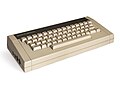
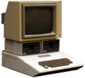
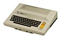
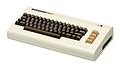
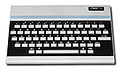
One of the first "public" uses for the design was the Apple I microcomputer, introduced in 1976. The 6502 was next used in the Commodore PET and the Apple II,[68] both released in 1977. It was later used in the Atari 8-bit computers, Acorn Atom, BBC Micro,[68] VIC-20 and other designs both for home computers and business, such as Ohio Scientific and Oric computers. The 6510, a direct successor of the 6502 with a digital I/O port and a tri-state address bus, was the CPU utilized in the best-selling[69][70] Commodore 64 home computer.
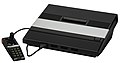
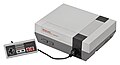
Another important use of the 6500 family was in video games. The first to make use of the processor design was the 1977 Atari VCS, later renamed the Atari 2600. The VCS used a 6502 variant named the 6507, which had fewer pins, so it could address only 8 KB of memory. Millions of the Atari consoles would be sold, each with a MOS processor. Another significant use was by the Nintendo Entertainment System and Famicom. The 6502 used in the NES was a second source version by Ricoh, a partial system on a chip, that lacked the binary-coded decimal mode but added 22 memory-mapped registers and on-die hardware for sound generation, joypad reading, and sprite list DMA. Called 2A03 in NTSC consoles and 2A07 in PAL consoles (the difference being the clock frequency divider ratio and a lookup table for audio sample rates), this processor was produced exclusively for Nintendo.
6502 or variants were used in all of Commodore's floppy disk drives for all of their 8-bit computers, from the PET line through the Commodore 128D, including the Commodore 64. 8-inch PET drives had two 6502 processors. Atari used the same 6507 used in the Atari VCS for its 810 and 1050 disk drives used for all of their 8-bit computer line, from the 400/800 through the XEGS.
In the 1980s, a popular electronics magazine Elektor/Elektuur used the processor in its microprocessor development board Junior Computer.
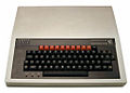
The CMOS successor to the 6502, the WDC 65C02, also saw use in home computers and video game consoles. Apple used it in the Apple II line starting with the Apple IIc and later variants of the Apple IIe and also offered a kit to upgrade older IIe systems with the new processor.[71] The Hudson Soft HuC6280 chip used in the TurboGrafx-16 was based on a 65C02 core. The Atari Lynx used a custom chip named "Mikey"[72] designed by Epyx which included a VLSI VL65NC02 licensed cell. The G65SC12 by GTE Microcircuits (renamed California Micro Devices) variant was used in the BBC Master. Some models of the BBC Master also included an additional G65SC102 co-processor.
- Home computers and video game consoles using the 6502 or its variants
-

-
-

-
-

-

-
-

-
-

-

-

-
-

-
-

-

-

-
-

-

-
-

-


Technical description


| 15 | 14 | 13 | 12 | 11 | 10 | 9 | 8 | 7 | 6 | 5 | 4 | 3 | 2 | 1 | 0 | (bit position) |
| Main registers | ||||||||||||||||
| A | Accumulator | |||||||||||||||
| Index registers | ||||||||||||||||
| X | X index | |||||||||||||||
| Y | Y index | |||||||||||||||
| 0 | 0 | 0 | 0 | 0 | 0 | 0 | 1 | SP | Stack Pointer | |||||||
| Program counter | ||||||||||||||||
| PC | Program Counter | |||||||||||||||
| Status register | ||||||||||||||||
| N | V | - | B | D | I | Z | C | Processor Flags | ||||||||
The 6502 is a little-endian 8-bit processor with a 16-bit address bus. The original versions were fabricated using an 8 µm[73] process technology chip with a die size of 3.9 mm × 4.3 mm (153 by 168 mils), for a total area of 16.6 mm2.[38]
The internal logic runs at the same speed as the external clock rate. It featured a simple pipeline; on each cycle, the processor fetches one byte from memory and processes another. This means that any single instruction can take as few as two cycles to complete, depending on the number of operands that instruction uses. For comparison, the Zilog Z80 required two cycles to fetch memory, and the miminum instruction time was four cycles. Thus, despite the lower clock speeds compared to competing designs, typically in the neighborhood of 1 to 2 MHz, the 6502's performance was competitive with CPUs using significantly faster clocks. This is partly due to a simple state machine implemented by combinational (clockless) logic to a greater extent than in many other designs; the two-phase clock (supplying two synchronizations per cycle) could thereby control the machine cycle directly.
This design also led to one useful design note of the 6502, and the 6800 before it. Because the chip only accessed memory during certain parts of the clock cycle, and those cycles were indicated by the PHI2-low clock-out pin, other chips in a system could access memory during those times when the 6502 was off the bus. This was sometimes known as "hidden access". This technique was widely used by computer systems; they would use memory capable of access at 2 MHz, and then run the CPU at 1 MHz. This guaranteed that the CPU and video hardware could interleave their accesses, with a total performance matching that of the memory device. Because this access was every other cycle, there was no need to signal the CPU to avoid using the bus, making this sort of access easy to implement without any bus logic. [74] When faster memories became available in the 1980s, newer machines could use this same technique while running at higher clock rates, the BBC Micro used newer RAM that allowed its CPU to run at 2 MHz while still using the same bus sharing techniques.
Like most simple CPUs of the era, the dynamic NMOS 6502 chip is not sequenced by microcode but decoded directly using a dedicated PLA. The decoder occupied about 15% of the chip area. This compares to later microcode-based designs like the Motorola 68000, where the microcode ROM and decoder engine represented about a third of the gates in the system.
Registers
Like its precursor, the 6800, the 6502 has very few registers. They include[75]
A= 8-bit accumulator registerP= 7-bit status registerPC= 16-bit program counterS= 8-bit stack pointerX= 8-bit index registerY= 8-bit index register
This compares to a contemporaneous competitor, the Intel 8080, which likewise has one 8-bit accumulator and a 16-bit program counter, but has six more general-purpose 8-bit registers (which can be combined into three 16-bit pointers) and a larger 16-bit stack pointer.[77]
In order to make up somewhat for the lack of registers, the 6502 includes a zero page addressing mode that uses one address byte in the instruction instead of the two needed to address the full 64 KB of memory. This provides fast access to the first 256 bytes of RAM by using shorter instructions. For instance, an instruction to add a value from memory to the value in the accumulator would normally be three bytes, one for the instruction and two for the 16-bit address. Using the zero page reduces this to an 8-byte address, reducing the total instruction length to two bytes, and thus improving instruction performance.
The stack address space is hardwired to memory page $01, i.e. the address range $0100–$01FF (256–511). Software access to the stack is done via four implied addressing mode instructions, whose functions are to push or pop (pull) the accumulator or the processor status register. The same stack is also used for subroutine calls via the JSR (jump to subroutine) and RTS (return from subroutine) instructions and for interrupt handling.
Addressing
The chip uses the index and stack registers effectively with several addressing modes, including a fast "direct page" or "zero page" mode, similar to that found on the PDP-8, that accesses memory locations from addresses 0 to 255 with a single 8-bit address (saving the cycle normally required to fetch the high-order byte of the address)—code for the 6502 uses the zero page much as code for other processors would use registers. On some 6502-based microcomputers with an operating system, the operating system uses most of zero page, leaving only a handful of locations for the user.
Addressing modes also include implied (1-byte instructions); absolute (3 bytes); indexed absolute (3 bytes); indexed zero-page (2 bytes); relative (2 bytes); accumulator (1); indirect,x and indirect,y (2); and immediate (2). Absolute mode is a general-purpose mode. Branch instructions use a signed 8-bit offset relative to the instruction after the branch; the numerical range −128..127 therefore translates to 128 bytes backward and 127 bytes forward from the instruction following the branch (which is 126 bytes backward and 129 bytes forward from the start of the branch instruction). Accumulator mode uses the accumulator as an effective address and does not need any operand data. Immediate mode uses an 8-bit literal operand.
Indirect addressing
The indirect modes are useful for array processing and other looping. With the 5/6 cycle "(indirect),y" mode, the 8-bit Y register is added to a 16-bit base address read from zero page, which is located by a single byte following the opcode. The Y register is therefore an index register in the sense that it is used to hold an actual index (as opposed to the X register in the 6800, where a base address was directly stored and to which an immediate offset could be added). Incrementing the index register to walk the array byte-wise takes only two additional cycles. With the less frequently used "(indirect,x)" mode the effective address for the operation is found at the zero page address formed by adding the second byte of the instruction to the contents of the X register. Using the indexed modes, the zero page effectively acts as a set of up to 128 additional (though very slow) address registers.
The 6502 is capable of performing addition and subtraction in binary or binary-coded decimal. Placing the CPU into BCD mode with the SED (set D flag) instruction results in decimal arithmetic, in which $99 + $01 would result in $00 and the carry (C) flag being set. In binary mode (CLD, clear D flag), the same operation would result in $9A and the carry flag being cleared. Other than Atari BASIC, BCD mode was seldom used in home-computer applications.
See the Hello world! article for a simple but characteristic example of 6502 assembly language.
Instructions and opcodes
6502 instruction operation codes (opcodes) are 8 bits long and have the general form AAABBBCC, where AAA and CC define the opcode, and BBB defines the addressing mode.[78]
For instance, consider the ORA instruction, which performs a bitwise OR on the bits in the accumulator with another value. The instruction opcode is of the form 000bbb01, where bbb may be 010 for an immediate mode value (constant), 001 for zero-page fixed address, 011 for an absolute address, and so on.[78]
This pattern is not absolute, and there are a number of exceptions. However, where it does apply, it allows one to easily deconstruct opcode values back to assembly mnemonics for the majority of instructions, handling the edge cases with special-purpose code.[78]
Of the 256 possible opcodes available using an 8-bit pattern, the original 6502 uses 151 of them, organized into 56 instructions with (possibly) multiple addressing modes. Depending on the instruction and addressing mode, the opcode may require zero, one or two additional bytes for operands. Hence 6502 machine instructions vary in length from one to three bytes.[79][80] The operand is stored in the 6502's customary little-endian format.
The 65C816, the 16-bit CMOS descendant of the 6502, also supports 24-bit addressing, which results in instructions being assembled with three-byte operands, also arranged in little-endian format.
The remaining 105 opcodes are undefined. In the original design, instructions where the low-order 4 bits (nibble) were 3, 7, B or F were not used, providing room for future expansion. Likewise, the $2x column had only a single entry, LDX #constant. The remaining 25 empty slots were distributed. Some of the empty slots were used in the 65C02 to provide both new instructions and variations on existing ones with new addressing modes. The $Fx instructions were initially left free to allow 3rd-party vendors to add their own instructions, but later versions of the 65C02 standardized a set of bit manipulation instructions developed by Rockwell Semiconductor.
Assembly language
A 6502 assembly language statement consists of a three-character instruction mnemonic, followed by any operands. Instructions that do not take a separate operand but target a single register based on the addressing mode combine the target register in the instruction mnemonic, so the assembler uses INX as opposed to INC X to increment the X register.
Instruction table
| Opcode matrix for the 6502 instruction set | ||||||||||||
|---|---|---|---|---|---|---|---|---|---|---|---|---|
| Addressing modes: A – accumulator, # – immediate, zpg – zero page, abs – absolute, ind – indirect, X – indexed by X register, Y – indexed by Y register, rel – relative | ||||||||||||
| High nibble | Low nibble | |||||||||||
| 0 | 1 | 2 | 4 | 5 | 6 | 8 | 9 | A | C | D | E | |
| 0 | BRK | ORA (ind,X) | ORA zpg | ASL zpg | PHP | ORA # | ASL A | ORA abs | ASL abs | |||
| 1 | BPL rel | ORA (ind),Y | ORA zpg,X | ASL zpg,X | CLC | ORA abs,Y | ORA abs,X | ASL abs,X | ||||
| 2 | JSR abs | AND (ind,X) | BIT zpg | AND zpg | ROL zpg | PLP | AND # | ROL A | BIT abs | AND abs | ROL abs | |